")
")
")
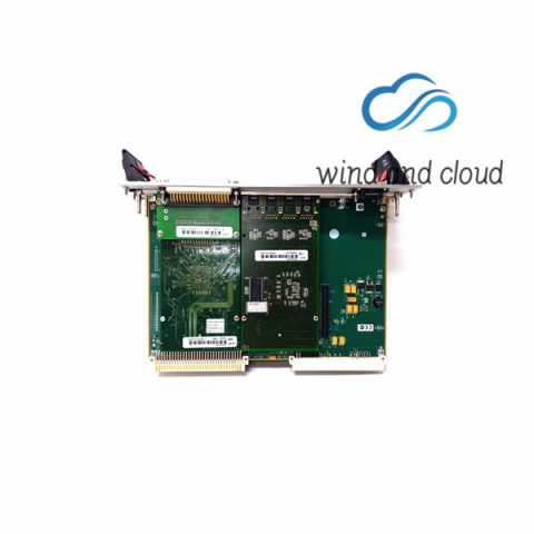
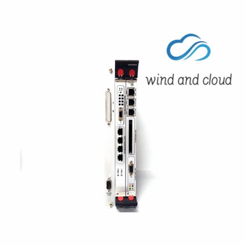

This chapter briefly describes the board level hardware features of the MVME6100 single board computer, including a table of features and a block diagram. The remainder of the chapter provides memory map information including a default memory map, MOTLoad’s processor memory map, a default PCI memory map, MOTLoad’s PCI memory map, a PCI I/O memory map, and system I/O memory maps.

REF_CLK Reference clock. This bit reflects the current state of the 28.8 KHz reference clock derived from the 1.8432 MHz UART oscillator divided by 64. This clock may be used as a fixed timing reference. BANK_SEL Boot Flash bank select. This bit reflects the current state of the boot Flash bank select jumper. A cleared condition indicates that Flash bank A is the boot bank. A set condition indicates that Flash B is the boot bank. SAFE_START ENV safe start. This bit reflects the current state of the ENV safe start select jumper. A set condition indicates that MOTLoad should provide the user the capability to select which Boot Image is used to boot the board, cleared MOTLoad should proceed with the first boot image found. ABORT_L Abort.
This bit reflects the current state of the on-board abort signal. This is a debounced version of the abort switch and may be used to determine the state of the abort switch. A set condition indicates that the abort switch is not depressed while a cleared condition would indicate that the abort switch is asserted. FLASH_BSY_L FLASH Busy. This bit provides the current state of the Flash Bank A StrataFlash device Status pins. These two open drain output pins are wire ORed. Refer to the appropriate Intel StrataFlash data sheet for a description on the function of the Status pin.
Software Flash Bank B Boot Block Write Protect. This bit is to provide software-controlled protection against inadvertent writes to the Flash Bank B Top 1 MB (0xFFF00000) space. Clearing this bit and disabling HW write-protect will enable writes to the Bank B Flash Top 1MB boot block devices. This bit is set during reset and must be reset by the system software to enable writing of the Flash Bank B boot block.
The MVME6100 board contains one EXAR ST16C554D Quad UART device connected to the MV64360 device controller bus to provide asynchronous debug ports. The Quad UART supports up to four asynchronous serial ports of which two are used on the MVME6100. The ST16C554D is a universal asynchronous receiver and transmitter and is an enhanced UART with 16 byte FIFOs, receive trigger levels, and data rates up to 1.5 Mbps. On-board status registers provide the user with error indications, operational status, and modem interface control. System interrupts may be tailored to meet user requirements. The ST16C554DCQ64 provides constant active interrupt outputs but do not offer TXRDY/RXRDY outputs. Refer to the EXAR ST16C554D data sheet for additional information.
There are no reviews yet.