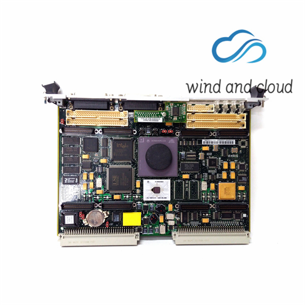
The VME162PA-252SE MK48T58 BBRAM (also called Non-Volatile RAM or NVRAM) is divided into six areas as shown in Table 1-15. The first five areas are defined by software, while the sixth area, the time-of-day (TOD) clock, is defined by the chip hardware. The first area is reserved for user data. The second area is used by Motorola networking software. The third area may be used by an operating system. The fourth area is used by the MVME172 board debugger (MVME172Bug). The fifth area, detailed in Table 1-16, is the configuration area. The sixth area, the TOD clock, detailed in Table 1-17, is defined by the chip hardware.
1.For a complete description of the register bits, refer to the data sheet for the specific chip. For a more detailed memory map, refer to the following detailed peripheral device memory maps.
2.The SCC is an 8-bit device located on an MC2 chip private data bus. Byte access is required.

3.Writes to the LCSR in the VMEchip2 must be 32 bits. LCSR writes of 8 or 16 bits terminate with a TEA signal. Writes to the GCSR may be 8, 16 or 32 bits. Reads to the LCSR and GCSR may be 8, 16 or 32 bits. Byte reads should be used to read the interrupt vector.
4.This area does not return an acknowledge signal. If the local bus timer is enabled, the access times out and is terminated by a TEA signal.
5.Size is approximate.
6.VME162PA-252SE Port commands to the 82596CA must be written as two 16- bit writes: upper word first and lower word second.
7.Not used.
8.To use this area, the ECC mezzanine board must be installed. If it is not installed, no acknowledge signal is returned; if the local bus timer is enabled, the access times out and is terminated by a TEA signal.
9.Repeats on 8KB boundaries.




There are no reviews yet.